What is BAT54S?
The BAT54S is a dual planar Schottky barrier diode for high-speed switching and low-forward voltage applications. It features integrated guard ring protection technology. Encapsulated in a SOT-23 (TO-236AB) surface-mounted package, the BAT54S is widely used in portable electronics.
BAT54S Working Principle
The operating principle of the BAT54S is based on the physical characteristics of a metal-semiconductor junction (Schottky barrier). Since it does not have the minority carrier storage effect found in traditional PN junction diodes, it offers an ultra-low forward voltage drop of only 0.3V–0.4V and an extremely fast reverse recovery time in the nanosecond (ns) range.
In practical circuits, when the input voltage exceeds the supply voltage or drops below the ground level, the corresponding diode instantly turns on in forward conduction mode, quickly diverting abnormal overvoltage or negative spike pulses to the power rail (VCC) or ground (GND).
BAT54S Specifications
Nexperia BAT54S,215 technical specifications is below.
Parameter | Value |
Part Number | BAT54S,215 |
Diode Type | Schottky |
Description | DIODE ARRAY SCHOTTKY 30V SOT23 |
Lead Free Status / RoHS Status | Lead free / RoHS Compliant |
Diode Configuration | 1 Pair Series Connection |
Series | Automotive, AEC-Q101 |
Operating Temperature - Junction | 150°C (Max) |
Reverse Recovery Time (trr) | 5ns |
Voltage - DC Reverse (Vr) (Max) | 30V |
Voltage - Forward (Vf) (Max) @ If | 800mV @ 100mA |
Mounting Type | Surface Mount |
Current - Reverse Leakage @ Vr | 2µA @ 25V |
Current - Average Rectified (Io) (per Diode) | 200mA (DC) |
Current Rating | 500mA |
Peak Reflow Temperature (Cel) | 260 |
Time@Peak Reflow Temperature-Max (s) | 30 |
Package | TO-236-3, SOT-23-3 |
Base Product Number | BAT54S |
BAT54S Pin Description
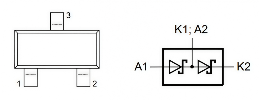
Pin 1 — A1: Anode terminal of diode 1.
Pin 2 — K2: Cathode terminal of diode 2.
Pin 3 — K1 / A2: Shared terminal functioning as the cathode of diode 1 and the anode of diode 2.
BAT54S Test Circuit
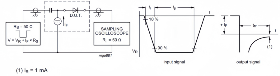
Reverse recovery time test circuit and waveforms
This figure shows the standard test circuit and waveform used to measure the reverse recovery time (trr) of the BAT54S.
In the test circuit on the left, the device under test (D.U.T.) is first driven with a forward current IF by a DC current source. Then, a fast reverse voltage pulse is applied by a pulse generator with an internal resistance of RS = 50Ω. Since Schottky diodes use a metal-semiconductor junction and do not have the minority carrier storage effect of standard PN junction diodes, only a very small reverse current spike appears when the signal quickly switches to reverse bias VR. As shown in the output waveform on the right, the reverse current rapidly decays to the specified threshold current IR = 1mA.
BAT54S Features
l Dual Schottky diodes integrated in one compact package.
l Ultra-small SOT-23 SMD package for easy PCB assembly.
l Nanosecond-level fast switching performance.
l Low forward voltage drop of about 0.35V–0.4V.
l Supports up to 30V reverse voltage.
l Maximum continuous forward current of 200mA.
l Surge current capability up to 600mA.
l Extremely low charge storage effect.
l Excellent overvoltage and ESD clamping performance.
l Available in AEC-Q101 automotive-grade versions.
l RoHS compliant and lead-free design.
BAT54S Applications
1. Ultra High-Speed Switching
Thanks to its nanosecond-level switching speed and low forward voltage drop, the BAT54S is widely used in high-frequency and fast-response switching circuits. It is suitable for RF circuits, signal routing, pulse detection, and high-speed digital communication systems.
2. Line Termination
The BAT54S can be used in line termination circuits to suppress signal reflections and improve signal integrity in high-speed data transmission systems. It is commonly applied in communication interfaces, data buses, and embedded electronic systems.
3. Voltage Clamping
The BAT54S is ideal for protecting sensitive I/O ports and low-voltage components from transient voltage spikes or electrostatic discharge (ESD). It is frequently used in USB ports, microcontroller interfaces, sensor inputs, and portable electronic devices.
4. Reverse Polarity Protection
The diode provides efficient reverse polarity protection with minimal power loss. It helps prevent damage caused by incorrect power supply connections in battery-powered products, industrial controllers, and consumer electronics.
BAT54S Equivalents
If you are looking for compatible alternatives for the BAT54S, the following models are commonly used in similar Schottky switching, clamping, and protection circuits:
l BAT54
l BAT54A
l BAT54C
l BAT54SDW
l BAT54T1G
BAT54 vs. BAT54S vs. BAT54A vs. BAT54C
These four models typically use a SOT-23-3 package, and their main difference lies in the internal diode pin configurations. The details are as follows:
Part Number | Internal Configuration | Topology Diagram Description | Critical Pin Features |
BAT54 | Single Diode | Contains only one independent diode internally. | Pin 1: Anode Pin 1: NC(Not Connected) Pin 3: Cathode
|
BAT54S | Series Pair | Two diodes connected in series; the cathode of D1 and the anode of D2 meet at the center pin. | Pin 1: Anode of D1 Pin 2: Cathode of D2 Pin 3: Public Terminal(D1 Cathode/D2 Anode)
|
BAT54A | Common Cathode | The cathodes (negative terminals) of both diodes are tied together. | Pin 1: Anode of D1 Pin 2: Anode of D2 Pin 3: Common Cathode
|
BAT54C | Common Anode | The anodes (positive terminals) of both diodes are tied together. | Pin 1: Cathode of D1 Pin 2: Cathode of D2 Pin 3: Common Anode
|
How to Use BAT54S Diode?
In practical circuit design, the BAT54S is often used for overvoltage clamping and ESD protection on high-speed signal lines or I/O ports.
In a typical connection, Pin 3 (common node) is connected to the protected signal line (e.g., MCU I/O, SPI, or I2C bus), Pin 1 is tied to GND, and Pin 2 is connected to the supply rail (e.g., 3.3V VCC).
When a positive voltage spike or ESD event occurs, once the signal exceeds VCC + 0.35V, the upper diode conducts and diverts excess energy to the power rail. Similarly, when a negative spike below about -0.3V appears, the lower diode conducts and clamps it to ground.
BAT54S Package
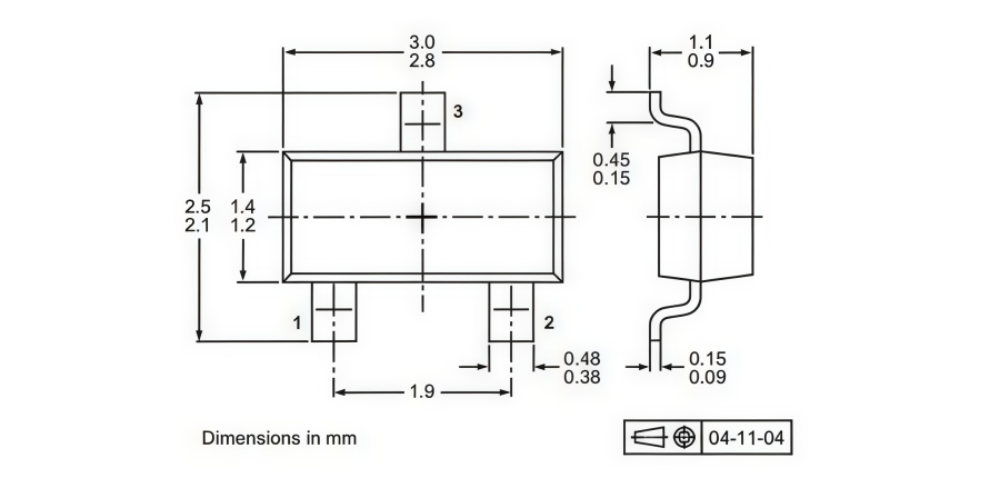
Here is the BAT54S package outline.
ANDE Electronics: Your Trusted Partner in Electronic Component Sourcing
At ANDE Electronics, we make getting the electronic components you need simple and fast. We work directly with top global manufacturers to provide high-quality components that have passed our strict checks, so you can count on them for your projects.
We also focus on quick and consistent delivery to keep your work on schedule and avoid delays. When you need reliable and efficient electronic parts for your projects, ANDE Electronics is a partner you can trust.