26/06/15
Innolux G150XGE-L04 Datasheet, Specs & Industrial Uses
The G150XGE-L04 is a 15-inch TFT-LCD display module developed by Innolux, primarily designed for industrial applications. It features an LED backlight system and an industrial-grade structural design, enabling stable and reliable long-term operation.This module is widely used in industrial automation equipment, Human-Machine Interface (HMI) terminals, control systems, and various industrial display platforms. This article provides a systematic overview of the G150XGE-L04, covering its specifications, features, interface structure, and industrial applications, helping engineers and procurement teams quickly understand its performance advantages and selection reference. G150XGE-L04 OverviewThe Innolux G150XGE-L04 is a 15.0-inch TFT-LCD display module featuring an LED backlight system and a 20-pin LVDS interface. It supports a resolution of 1024×768 (XGA) and displays 16.2 million or 262,000 colors; offering stable image output and excellent display consistency, it is suitable for a wide range of industrial display applications.Designed in accordance with PSWG standards, the module features industry-standard mechanical and electrical interface configurations, facilitating system compatibility and ease of replacement. Additionally, the integration of the backlight driver circuit onto the PCBA simplifies system design, making it ideal for industrial control and embedded display equipment.(Contact us for a quote) G150XGE-L04 Technical SpecificationsThis section outlines the key technical specifications of the G150XGE-L04, providing a comprehensive overview of its performance. The table below lists the specifications for this LCD panel:Parameter ValueBrandInnoluxModelG150XGE-L04Size15"CompositionLCMResolution1024(RGB)×768, XGA 85PPILuminance400 cd/m² (Typ.)Contrast Ratio700 : 1 (Typ.) (TM)Viewangle80/80/70/70Color Depth262K/16.2M 55% NTSCLight SourceWLED , 50K hours , With LED DriverInterface TypeLVDS (1 ch, 6/8-bit) , 20 pins ConnectorActive Area307.4(W)×231.3(H) mmPixel FormatRGB Vertical StripeFrame Rate60HzTouchscreenWithoutVoltage Supply3.3V (Typ.)Weight835g (Typ.)Outline Size326.5(H)×253.5(V)×12(D) mmMax RatingsOperating Temperature: -30 ~ 80 °C ; Storage Temperature: -40 ~ 85 °C Refer to G150XGE-L04 Datasheet PDF G150XGE-L04 Pin ConfigurationThis module adopts an LVDS (1-channel, 6-bit/8-bit compatible) signal interface. The display data and logic signals are transmitted through a 20-pin surface-mount connector, with the commonly used matching socket typically being MSB240420-E. When designing the carrier board, it is necessary to select a precisely compatible cable harness and wiring assembly.Pin No.SymbolFunction1VCCPower Supply +3.3V(typical)2VCCPower Supply +3.3V(typical)3GNDGround4LR/UDReverse Scan Control H or NC = Normal Mode. L = Horizonta/ Vertical Reverse Scan.5RX0-LVDS Differential Data Input6RX0+LVDS Differential Data Input7GNDGround8RX1-LVDS Differential Data Input9RX1+LVDS Differential Data Input10GNDGround11RX2-LVDS Differential Data Input12RX2+LVDS Differential Data Input13GNDGround14RXCLK-LVDS Differential Data Input15RXCLK+LVDS Differential Data Input16GNDGround17RX3-LVDS Differential Data Input18RX3+LVDS Differential Data Input19GNDGround20SEL68LVDS 6/8 bit select function control, High → 6bit Input Mode Low or NC → 8bit Input Mode Hardware TipsTo avoid signal distortion or hardware damage, PCB engineers must strictly follow the two rules below during layout design: 1. 100Ω Differential Impedance Control LVDS signals (such as RX0±) are high-speed differential signals, and the trace impedance must be controlled at 100Ω ±10%. Differential pairs must be strictly length-matched (within ±5 mil), via usage should be minimized, and a solid ground reference plane should be provided to reduce reflection and EMI, preventing screen flickering or water ripple effects. 2. Strict Power On/Off Sequence ControlDuring power-up, VCC (e.g., 3.3V) must be stabilized first, and after meeting the required delay (typically Tt > 0.5 ms), LVDS signals can be enabled. During power-down, LVDS signals must be disabled first before cutting off VCC. Otherwise, the driver IC may enter a latch-up condition, causing excessive current and potential damage to the module.(Contact us for a quote) G150XGE-L04 Block Diagram AnalysisAccording to the system block diagram, the G150XGE-L04 module completes image display through four main paths: signal decoding, power conversion, row/column driving, and independent backlight control.First, external LVDS differential signals and clock are transmitted through the 20-pin connector to the LVDS receiver for image decoding. Meanwhile, the input logic voltage VCC is converted by a DC/DC converter into internal reference voltages required by each circuit block.Next, the decoded timing data is sent to the scan driver IC (row driver) and data driver IC (column driver) to accurately control the 1024 × 768 TFT LCD panel. At the same time, independent backlight power (Vi) is supplied via a 5-pin connector and regulated by the built-in LED converter, providing a stable constant-current drive for the LED backlight unit. G150XGE-L04 Advantages and DisadvantagesThe G150XGE-L04 LCD display offers multiple key advantages, but it also has certain potential limitations. We will help engineers evaluate its suitability in a more comprehensive and objective way. Prosl Supports a wide operating temperature range of -30 ~ 80°C, making it suitable for harsh industrial environments.l Offers long backlight life (≥50,000 hours), ensuring stable long-term operation.l It features a built-in LED driver, simplifying system design and improving power stability.l Supports up to 1.5G vibration resistance, making it reliable in mechanical and mobile applications.l Adopts LVDS interface with 6/8-bit support, providing flexible system compatibility.l Follows PSWG standards, ensuring better interchangeability and industrial compatibility.l Uses WLED backlight technology for efficient and uniform brightness performance.l Features a matte anti-glare surface, improving readability in bright industrial lighting conditions.l Supports lamp-replaceable design, reducing long-term maintenance cost and downtime. Consl It does not include a touch panel, requiring an additional touch solution for interactive applications.l Uses XGA (1024×768) resolution, which is lower than modern Full HD display standards.l Limited color depth flexibility in 6-bit/8-bit modes compared to higher-end displays.l Designed mainly for industrial use, making it less suitable for high-end multimedia or consumer display applications.(Contact us for a quote) Typical Applications in Industrial FieldsBased on the features and advantages of the G150XGE-L04 LCD panel, it is widely used in the industrial field, The screen is suitable for the industrial application scenarios below. 1. Industrial Automation SystemsThe G150XGE-L04 is widely used in human-machine monitoring interfaces on industrial automation production lines for real-time monitoring of equipment status and production data.l PLC control panelsl Automated assembly line terminalsl Smart factory monitoring displays 2. Human-Machine Interface (HMI) SystemsThis module is commonly used as the core display in industrial HMI systems, serving as the interactive interface between operators and equipment, supporting stable long-term operation.l Equipment parameter setting terminalsl Machine tool operation panels 3. Medical Industrial Equipment Display SystemsThe G150XGE-L04 is used in medical equipment to provide stable and clear operational display interfaces, suitable for environments requiring high reliability.l Patient monitorsl Ultrasound diagnostic equipment 4. Test & Measurement EquipmentThe G150XGE-L04 is widely used in various industrial testing instruments, providing clear and stable data visualization interfaces.l Oscilloscope displaysl Industrial inspection equipmentl Laboratory data acquisition systems 5. Embedded Industrial Computing SystemsThis module is suitable for various embedded control systems as a core display output device.l Industrial PCsl Edge computing terminals ANDE Electronics: Reliable LCD Display SolutionsAs a professional display supplier, Ande Electronics is committed to providing LCD modules that meet modern application needs.We offer not only high-quality display products but also reliable technical support and flexible purchasing options. Our experienced engineering team works closely with customers to provide guidance on module selection, integration, and optimization.Choosing Ande Electronics, then engineers and manufacturers will gain a partner focused on quality, innovation, and efficiency.(Contact us for a quote)
324

26/06/12
Innolux G156BGE-L01 15.6'' LCD Guide & Datasheet
G156BGE-L01 IntroductionInnolux G156BGE-L01 is a 15.6-inch industrial-grade a-Si TFT-LCD display module designed for industrial applications. The display features a WXGA (1366 × 768) resolution and supports up to 16.7 million colors, meeting the display quality and information visualization requirements of industrial equipment.The G156BGE-L01 integrates a WLED backlight system and includes a built-in backlight driver circuit (Converter Module). The module adopts a standard 30-pin single-channel LVDS (1ch-LVDS) interface, providing good compatibility and enabling easy connection with industrial motherboards and various display controllers. G156BGE-L01 StructureThe G156BGE-L01 LCD panel adopts a classic flat rectangular industrial-grade design. Its overall outline dimensions are 363.8 (W) × 215.92 (H) mm, with a thickness of 16.85 ± 0.5 mm. Featuring a robust metal frame structure and vibration-resistant design (up to 1.5G), it effectively protects its 344.232 × 193.536 mm active display area.The front surface of the module is treated with an anti-glare matte finish and a 3H hard-coating layer. Meanwhile, the rear side integrates an edge-lit WLED backlight unit and a built-in LED driver. Standard side and rear mounting holes are provided on the housing, making the module highly convenient for stacking and fixed installation. G156BGE-L01 Key SpecificationsThis section provides a detailed overview of the key technical specifications of the Innolux G156BGE-L01, including electrical characteristics, mechanical specifications, and other important parameters, helping you evaluate this LCD panel more effectively.Parameter ValueBrandInnoluxModelG156BGE-L01Size15.6"CompositionLCMResolution1366(RGB)×768, WXGA 100PPILuminance300 cd/m² (Typ.)Contrast Ratio500 : 1 (Typ.) (TM)Viewangle80/80/80/80Color Depth16.7M 65% NTSCLight SourceWLED , 50K hours , With LED DriverInterface TypeLVDS (1 ch, 8-bit) , 30 pins ConnectorActive Area347.53(W)×196.84(H) mmPixel FormatRGB Vertical StripeFrame Rate60HzTouchscreenWithoutVoltage Supply5.0V (Typ.)Weight1.19/1.25Kgs (Typ./Max.)Outline Size363.8(H)×215.92(V) ×17.35(D) mmMax RatingsOperating Temperature: 0 ~ 60 °C ; Storage Temperature: -20 ~ 60 °C Refer to G156BGE-L01 Datasheet PDF G156BGE-L01 Interface and Pin ConfigurationThe following are the detailed pin definitions and function descriptions for the 30-pin LVDS interface of the Innolux G156BGE-L01 industrial LCD panel. This module typically uses a 30-pin connector with a 1.0 mm pitch, such as the P-TWO 187114-30091 or an equivalent connector. Pin Assignment Logic Drive Voltage:Unlike some low-voltage slim panels, the G156BGE-L01’s logic input voltage typically has a standard value of 5.0V. During hardware power management design, it is essential to provide a stable 5V power rail and ensure the supply current meets the typical requirement of 0.22A to 0.27A. Hardware Layout and Timing Considerations:When designing the wiring for embedded motherboards or driver boards, engineers must pay special attention to the LCD power-on and power-off sequence. If LVDS signals are applied before the 5V logic voltage is properly stabilized, or if signal voltage remains after the 5V supply is cut off, it may easily cause the panel driver ICs (Gate IC / Source IC) to suffer from latch-up effects, leading to overheating damage or even irreversible screen failure.Therefore, it is strongly recommended to implement strict timing delay control in firmware or hardware circuitry to ensure safe and stable operation throughout the device’s lifecycle. G156BGE-L01 Functional Block DiagramThe functional block diagram of the Innolux G156BGE-L01 shows a dual-path architecture for signal and power driving.The external mainboard provides Vcc power, ground, and LVDS differential signals (RX0–RX3 and clock RXC) through the 30-pin input interface. The Vcc is fed into a DC/DC converter and reference voltage circuit to generate internal operating voltages, while the LVDS signals are decoded by the timing controller (T-CON IC) for timing distribution. It then drives the scan driver IC and data driver IC to control the TFT LCD panel and display dynamic images.Meanwhile, the backlight section is powered through a separate connector, where the power is processed by a built-in driver circuit to activate the WLED backlight unit, providing the screen’s illumination source. Why G156BGE-L01 is Ideal for Industrial Applications?G156BGE-L01 features mature display performance and demonstrates significant advantages in industrial applications. The following sections analyze its industrial value from multiple aspects. 1. Industrial-Grade DurabilityG156BGE-L01 adopts an industrial-grade structural design, supporting vibration resistance up to 1.5G (14.7 m/s²) and offering strong electromagnetic interference (EMI) resistance. Its operating temperature range is 0 ~ 60°C, with a storage temperature range of -20 ~ 60°C, enabling reliable 24/7 continuous operation. 2. Long-Term AvailabilityAs an industrial TFT-LCD product, G156BGE-L01 offers a long product lifecycle and stable supply, effectively reducing the cost of system re-certification caused by frequent EOL (End of Life) issues. 3. Anti-Glare Surface TreatmentThe module features a front anti-glare matte surface and a 3H hardness coating, effectively reducing ambient light reflections and improving readability and operational accuracy. 4. Long-Life BacklightG156BGE-L01 uses a WLED backlight system with an integrated LED driver circuit. The backlight lifetime can reach ≥50,000 hours, helping reduce maintenance costs and improve overall system reliability. G156BGE-L01 Top Applications in Industrial FieldsThe G156BGE-L01 industrial panel flexibly adapts to various system platforms, providing clear and stable visual support for a wide range of terminal devices. Industrial Automation HMIThe G156BGE-L01 is widely used for Human-Machine Interfaces (HMIs) in industrial automation control systems, displaying real-time equipment operating status and parameter information.l PLC control panelsl Production line monitoring terminalsl Automation control cabinet displays Test & Measurement EquipmentIn various testing and inspection devices, this screen displays test data, waveforms, and analysis results, ensuring clear and stable data visualization.l Circuit testersl Automated Optical Inspection (AOI) equipmentl Signal analyzers Industrial Self-Service TerminalsIn various industrial-grade self-service systems, this panel provides stable HMI display capabilities, commonly serving as the interface for user operations and information display.l Self-service inquiry kiosksl Industrial POS systems Transportation SystemsWith its vibration resistance and wide operating temperature range, this panel is suitable for transportation and in-vehicle display systems, ensuring stable operation and reliable information display in complex environments.l Rail transit control screensl In-vehicle information terminalsl Bus dispatch systems Embedded Industrial SystemsThe G156BGE-L01 frequently serves as a display module for embedded systems, utilized in various industrial computing platforms and control devices to provide a standardized display solution.l Industrial embedded motherboardsl All-in-one industrial PCsl Intelligent edge computing devices Assembly And Handling Precautions (1) Do not apply rough force such as bending or twisting to the module during assembly.(2) To assemble or install module into user’s system can be only in clean working areas. The dust and oil may cause electrical short or worsen the polarizer.(3) It’s not permitted to have pressure or impulse on the module because the LCD panel and Backlight will be damaged.(4) Always follow the correct power sequence when LCD module is connecting and operating. This can prevent damage to the CMOS LSI chips during latch-up.(5) Do not pull the I/F connector in or out while the module is operating.(6) Do not disassemble the module.(7) Use a soft dry cloth without chemicals for cleaning, because the surface of polarizer is very soft and easily scratched.(8) It is dangerous that moisture come into or contacted the LCD module, because moisture may damage LCD module when it is operating.(9) High temperature or humidity may reduce the performance of module. Please store LCD module within the specified storage conditions.(10)When ambient temperature is lower than 10℃ may reduce the display quality. For example, the response time will become slowly. ANDE Electronics: Reliable LCD Display SolutionsAs a professional display supplier, Ande Electronics is committed to providing LCD modules that meet modern application needs.We offer not only high-quality display products but also reliable technical support and flexible purchasing options. Our experienced engineering team works closely with customers to provide guidance on module selection, integration, and optimization.Choosing Ande Electronics, then engineers and manufacturers will gain a partner focused on quality, innovation, and efficiency.(Contact us for a quote)
376
26/06/10
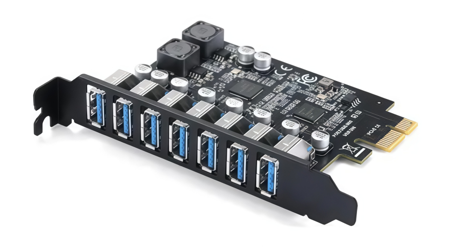
USB-to-Serial & USB HUB Chips Solutions | WCH Alternatives
With the rapid development of industrial automation, consumer electronics, medical devices, communication equipment, and the Internet of Things (IoT) industry, the USB interface has become an indispensable data transmission and connectivity standard in modern electronic products. Whether it is USB-to-serial communication or USB hub port expansion, related interface chips play a critical role in device interconnection, data exchange, and system control, with continuously growing market demand.At the same time, driven by global supply chain adjustments, rising prices of imported chips, and fluctuations in delivery cycles, an increasing number of companies are turning their attention to domestic USB interface chip solutions. Compared with imported products, domestic solutions not only effectively reduce procurement costs, but also offer advantages such as stable supply, controllable lead times, and localized technical support. This article will focus on USB-to-serial chips and USB hub controller chips, and introduce the application advantages and selection directions of their alternative solutions.(Contact us for a quote) What is a USB-to-Serial Chip?A USB-to-Serial chip (USB to UART Bridge IC) is an interface device that enables conversion between USB interfaces and serial communication protocols. Its core function is to convert USB signals from a computer into traditional serial communication signals (such as UART or TTL levels), thereby enabling stable communication between modern USB-based devices and embedded systems. This type of chip is widely used in microcontroller development boards, industrial control equipment, debugging tools, and various embedded systems. 1. Working Principle of USB-to-Serial ChipsThe operation of a USB-to-Serial chip is essentially a process of “protocol conversion + data buffering + level adaptation.” When a computer sends data via the USB interface, the internal controller of the chip first parses the USB protocol packets and converts them into serial communication data (UART format), which is then output through TX/RX pins to the target device.In the reverse direction, UART data transmitted from the serial device is repackaged into USB data packets by the chip and sent back to the computer via the USB interface, enabling bidirectional communication. 2. USB and UART Protocol ConversionThe USB protocol is a complex host-controlled high-speed communication protocol, whereas UART is a simple asynchronous serial communication method. The key function of a USB-to-Serial chip is to seamlessly bridge these two fundamentally different communication mechanisms:l USB side: responsible for device enumeration, data packet encapsulation, and high-speed communication with the PC hostl UART side: responsible for simple, low-speed, point-to-point communication with MCUs or peripheral devicesThrough an internal protocol conversion engine, the chip converts USB data streams into standard UART frame formats (start bit, data bits, parity bit, stop bit), enabling cross-protocol communication. 3. Enabling Communication Between PC and MCUIn embedded development, USB-to-Serial chips serve as the most common communication bridge between PCs and MCUs (microcontrollers). Developers can use serial terminal tools on a computer to directly interact with MCUs, enabling:l Firmware downloading and upgradingl Real-time data monitoringl Command transmission and response feedbackl System status debuggingThis communication method is simple, stable, and cost-effective, making it an essential tool in engineering development.(Contact us for a quote) USB-to-Single-Serial Port Chip SolutionThe USB-to-single-serial port chip solution integrates a USB interface and a single UART channel into one chip, enabling an efficient and compact communication architecture. This solution helps reduce overall BOM cost and is compatible with mainstream operating systems such as Windows, Linux, and macOS, without requiring complex driver adaptation.This solution is mainly used in:l MCU development boardsl Industrial controllersl Smart home devicesl Portable testing equipmentl Communication terminals USB-to-Dual-Serial Port Chip SolutionThe USB-to-dual-serial port chip solution enables multiple UART channels to be expanded through a single USB interface, supporting a multi-device communication architecture. By managing multiple serial ports through a unified USB host interface, it helps optimize data transmission structure and improve communication efficiency.This solution is widely used in:l Industrial gatewaysl Serial serversl Data acquisition systemsl Smart communication terminals USB-to-Quad-Serial Port Chip SolutionThe USB-to-quad-serial port chip solution is designed for multi-serial parallel communication requirements. It expands four independent UART channels through a single USB interface, meeting the needs of complex systems requiring synchronized multi-device communication and concurrent data processing. At the same time, a centralized USB management architecture further improves communication latency and system stability.This solution is mainly used in:l PLC control systemsl Industrial automation equipmentl Robotics control platformsl Test and measurement equipmentl Edge computing terminals WCH USB-to-Serial Chip SolutionsWCH provides a complete and mature USB-to-serial chip portfolio, covering single-channel, multi-channel, and high-integration application requirements. Its cost-effective USB-to-UART product families include CH9102X, CH342F, CH9104L, and other series, supporting industrial control and multi-node data communication applications.These models serve as ideal replacements for various imported USB-to-serial chips (such as FT232 and CP2102), helping customers achieve stable supply and localized supply chain optimization.(Contact us for a quote) What is a USB HUB Controller Chip?A USB HUB controller chip is a core device used to expand the number of available USB interfaces. It can convert a single USB host port into multiple USB downstream ports, enabling simultaneous connection and communication with multiple devices. As a fundamental component for USB interface expansion and device interconnection, USB HUB chips are widely used in computer peripherals, industrial equipment, and consumer electronics.The core function of a USB HUB chip is to centrally manage and distribute USB data traffic. It not only provides USB port expansion, but also handles data forwarding and traffic scheduling, ensuring stable operation of multiple peripheral devices under a single USB host controller. USB2.0 4-Port HUB SolutionThe USB2.0 4-port HUB solution provides four USB port expansion capabilities with plug-and-play functionality. It requires no complex driver configuration and offers strong system compatibility and stability, making it a cost-effective basic USB expansion solution.This solution is mainly used in:l Office equipmentl Printing devicesl Industrial control hostsl Educational electronic devices USB2.0 7-Port HUB SolutionThe USB2.0 7-port HUB solution is designed for higher-density multi-device connectivity requirements. It provides seven USB expansion ports, significantly enhancing peripheral device connectivity. This solution supports complex peripheral management and simultaneous multi-device operation.It is widely used in:l Industrial PCsl KVM devicesl Smart terminalsl Data center auxiliary equipment USB3.0 4-Port HUB SolutionThe USB3.0 4-port HUB solution is designed for high-speed data transmission applications. It provides four high-speed USB expansion ports, supports high-bandwidth data communication requirements, and is backward compatible with USB2.0 devices, balancing performance and compatibility.It is mainly used in:l Industrial vision systemsl AI edge computing devicesl Video capture systemsl Medical imaging equipmentl High-speed storage docking stations(Contact us for a quote) WCH USB HUB Controller Chip SolutionsWCH provides a complete USB HUB product portfolio, covering both USB2.0 and USB3.0 multi-port expansion solutions with strong stability and cost advantages, including CH334Q, CH338X, CH634W6T, etc.These chips serve as ideal replacements for various imported USB HUB controller solutions and are widely used in consumer electronics, industrial control, and embedded system applications. Ande Electronics: Providing USB Interface IC SolutionsAnde Electronics focuses on providing high-performance IC solutions, including core products such as USB-to-Serial chips and USB HUB controller chips, delivering stable and reliable interface connectivity solutions for customers.In addition, we primarily offer the full range of USB interface ICs from WCH, including USB-to-Serial and USB HUB solutions. These products feature strong compatibility and can meet the requirements of a wide variety of complex application scenarios.Ande Electronics supports Pin-to-Pin replacement solutions for mainstream imported chips, helping customers achieve rapid substitution and system upgrades. We also provide professional component selection support, alternative solution design, and stable supply services to ensure long-term supply chain security and project continuity.(Contact us for a quote)Replace Models.xlsx
251
26/06/05
DS2401 Silicon Serial Number IC 1-Wire Unique ID Chip
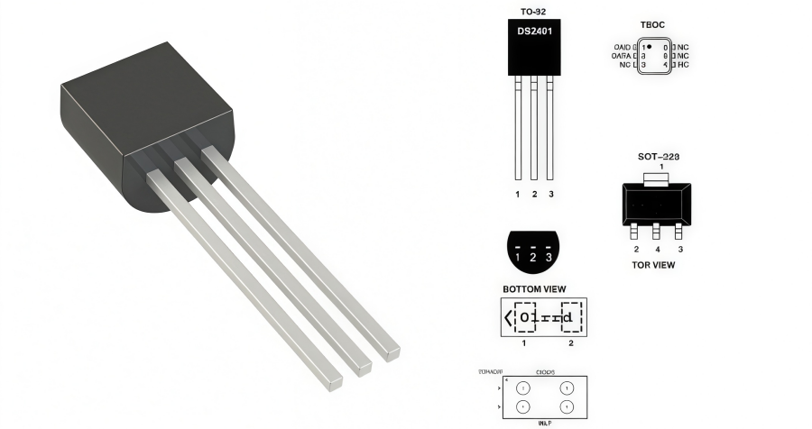
DS2401 DescriptionThe DS2401 is a low-cost silicon serial number IC designed to provide an absolutely unique electronic identity for products, systems, and embedded equipment. It integrates a factory-programmed 64-bit ROM, consisting of a unique 48-bit serial number, an 8-bit Family Code (01h), and an 8-bit CRC for data integrity verification. One of the key advantages of the DS2401 is its implementation of the 1-Wire communication protocol, which requires only a single data line and a ground connection for operation. The device is powered directly from the data line through parasitic power technology. As an enhanced successor to the DS2400, the DS2401 maintains full backward compatibility while adding multi-drop support, allowing multiple devices to share the same 1-Wire bus. (Contact us for a quote) DS2401 OperationThe DS2401’s internal ROM is accessed via a single data line. The 48-bit serial number, 8-bit family code and 8-bit CRC are retrieved using the 1-Wire protocol. This protocol defines bus transactions in terms of the bus state during specified time slots that are initiated on the falling edge of sync pulses from the bus controller. All data is read and written least significant bit first. DS2401 1-Wire Bus SystemThe 1-Wire bus is a system which has a single bus controller system and one or more peripherals. In all instances, the DS2401 is a peripheral device. The bus controller is typically a microcontroller. The discussion of this bus system is broken down into three topics: hardware configuration, transaction sequence, and 1-Wire signaling (signal type and timing). DS2401 Bus Controller CircuitOPEN DRAINSTANDARD TTLDS2401 Key SpecificationsBelow is the main technical specs about DS2401+.ParameterValuePart NumberDS2401+DescriptionIC SILICON SERIAL NUMBER TO92-3Lead Free Status / RoHS StatusLead free / RoHS CompliantTypeSilicon Serial NumberPart StatusActiveManufacturerAnalog Devices Inc./Maxim IntegratedCommunication Interface1-Wire®Power Supply Voltage2.8V – 6.0VOperating Temperature-40°C ~ +85°CMounting TypeThrough HolePackageTO-92-3Base Product NumberDS2401(Contact us for a quote) DS2401 Pin ConfigurationsPin 1: GND — GroundPin 2: Data / DQ — Bidirectional 1-Wire data input/output pin, also used for parasite power supply.Pin 3: NC (No Connection) — Internally not connected; typically left floating during PCB layout. DS2401 Features and Benefitsl Guaranteed Unique 64-Bit ROM ID Chip for Absolute Traceability- Unique, 64-Bit Registration Number (8-Bit Family Code + 48-Bit Serial Number + 8-Bit CRC Tester)- 8-Bit Family Code Specifies DS2401 Communications Requirements to Reader l Minimalist 1-Wire® Interface Lowers Cost and Interface Complexity- Multiple DS2401 Devices Can Reside on a Common 1-Wire Net- Built-In Multidrop Controller Ensures Compatibility with Other 1-Wire Net Products- Reduces Control, Address, Data, and Power to a Single Pin and Communicates at up to 16.3kbps- Presence Pulse Acknowledges When the Reader First Applies Voltage- Low-Cost TO-92, SOT-223, and TSOC Surface-Mount Packages- TO-92 Tape-and-Reel Version with Leads Bent to 100-mil Spacing (Default) or with Straight Leads (DS2401-SL) l Wide Voltage and Temperature Operating Ranges Enables Robust System Performance- Extended 2.8V to 6.0V Range (DS2401)- Zero Standby Power Required- -40°C to +85°C Industrial Temperature Range(Contact us for a quote) DS2401 ApplicationsDS2401 provides a low-cost, non-replicable, and configuration-free hardware-level unique ID system. Therefore, it is widely used as a fundamental identification solution in PCB management, device tracking, network node identification, product authentication, and embedded system management. 1. PCB Identification DS2401 is commonly soldered onto PCBs to serve as a unique hardware identity (Hardware ID) for each circuit board.l Unique board-level identification at production stagel SMT manufacturing traceability managementl Binding of test data to specific boardsl Repair and return tracking for lifecycle management 2. Network Node ID In distributed systems and industrial networks, DS2401 is used as a unique identity source for network nodes, enabling differentiation between devices or communication nodes.l IoT device network identity assignmentl Distributed sensor network node numberingl Edge computing device identity management 3. Equipment RegistrationDS2401 is widely used in equipment registration and asset management systems as a hardware-based “digital identity card” for devices.l Asset onboarding and warehouse registrationl Equipment lifecycle tracking and managementl Maintenance and service record bindingl Prevention of duplicate or counterfeit registration 4. Product AuthenticationDS2401 serves as a hardware-based anti-counterfeiting chip used to verify whether a product is genuine and factory-original.l Original spare parts verificationl Anti-counterfeit identification systemsl Hardware-based software licensing bindingl Authentication of high-value products 5. Embedded System Identification (System-Level ID) In embedded systems, DS2401 functions as a system-level unique hardware identifier used to distinguish individual device instances.l Industrial control boards (MCU / PLC systems)l IoT terminal device identity bindingl Firmware authorization and device lockingl Cloud-based device provisioning and registration(Contact us for a quote) Reading Serial from DS-2401 Using Arduino Uno FAQsWhat is DS2401+?The DS2401 is a silicon serial number device designed to provide a permanently programmed and globally unique 64-bit identification code. The “+” suffix does not indicate any functional difference; it simply identifies the newer RoHS-compliant, lead-free version of the device. The DS2401+ meets current environmental and regulatory requirements for lead-free electronic components.What is DS2401 used for?DS2401 is mainly used as a unique electronic identification chip for devices and systems. It provides a factory-programmed 64-bit ID, making it ideal for PCB identification, asset tracking, network node ID, and product authentication.Can multiple DS2401 devices share the same bus?Yes. DS2401 supports multi-drop 1-Wire communication, allowing multiple devices to operate on a single data line without address conflicts. ANDE Electronics: Your Trusted Partner in Electronic Component SourcingAt ANDE Electronics, we make getting the electronic components you need simple and fast. We work directly with top global manufacturers to provide high-quality components that have passed our strict checks, so you can count on them for your projects.We also focus on quick and consistent delivery to keep your work on schedule and avoid delays. When you need reliable and efficient electronic parts for your projects, ANDE Electronics is a partner you can trust.(Contact us for a quote)
293
26/06/02
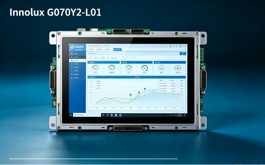
Innolux G070Y2-L01 7'' Industrial & Automotive LCD Panel
G070Y2-L01 is a 7-inch TFT Liquid Crystal Display module with an LED backlight unit and a 20pin 6/8bit LVDS interface controller board. The converter for the LED Backlight Unit is built in. This module supports 800 (R.G.B )x 480 WVGA mode, whose main application is the automotive display and industrial field. This article provides an overview of the G070Y2-L01, helping engineers and procurement professionals better understand its technical advantages and application value. As a display solutions supplier, Ande Electronics can also provide sourcing and technical support services for industrial display products, including the G070Y2-L01.(Contact us for a quote) G070Y2-L01 General SpecsAfter understanding the basics of the G070Y2-L01, its core specifications serve as important factors for evaluating product performance and system compatibility. The following section outlines the key specifications of this display module.Parameter ValueBrandInnoluxModelG070Y2-L01Size7"CompositionLCMResolution800(RGB)×480, WVGA 133PPILuminance500 cd/m² (Typ.)Contrast Ratio600 : 1 (Typ.) (TM)Viewangle70/70/60/60Color Depth262K/16.2M 72% NTSCLight SourceWLED , 50K hours , With LED DriverInterface TypeLVDS (1 ch, 6/8-bit) , 20 pins ConnectorActive Area154.6(W)×93.64(H) mmPixel FormatRGB Vertical StripeFrame Rate60HzTouchscreenWithoutVoltage Supply3.3V (Typ.)Weight147/162g (Typ./Max.)Outline Size165(W)×104(H) ×9.83(D) mmVibration Level3.0G (29.4 m/s²)Max RatingsOperating Temperature: -30 ~ 85 °C ; Storage Temperature: -40 ~ 95 °C Refer to G070Y2-L01 Datasheet PDF G070Y2-L01 Electrical & Signal InterfaceThe signal architecture and electrical control design of the Innolux G070Y2-L01 are well suited for industrial control and automotive electronics applications. 1. LVDS InterfaceThe G070Y2-L01 natively adopts a 20-pin single-channel (1-ch) LVDS interface. This interface offers low electromagnetic interference (EMI) and strong noise immunity while supporting both 6-bit and 8-bit digital signal input modes:l 6-bit Mode (262K Colors):When configured in 6-bit mode, the data transmission path is simplified, helping reduce overall system power consumption.l 8-bit Mode (16.2M Colors):For applications requiring higher color quality and minimal color banding, the module utilizes built-in FRC (Frame Rate Control) technology to achieve up to 16.2 million display colors for smoother and more realistic image rendering. 2. LVDS Differential Pair Layout GuidelinesTo ensure reliable high-speed signal transmission, the following PCB layout recommendations should be followed:1) Differential Impedance ControlAll five differential pairs (Channel 0, Channel 1, Channel 2, Channel 3, and CLK) should maintain a differential impedance of 100Ω ±10%.2) Length Matching Requirementsl Within each differential pair (such as RX0+ and RX0−), the length mismatch should be controlled within 5 mil.l Between different channels (such as Channel 0 and CLK), the length mismatch should be controlled within 20 mil.3) Routing RecommendationsDifferential pairs should be routed on the same signal layer whenever possible, and the use of excessive vias should be minimized to reduce signal reflections and timing jitter.(Contact us for a quote) G070Y2-L01 Features and BenefitsThis section focuses on the key features and advantages of the G070Y2-L01 LCD module of its performance, helping to more intuitively evaluate its operating performance across different systems.l Wide Operating Temperature Range: Supports -30°C to 85°C operation and -40°C to 95°C storage.l High Reliability for Industrial Use: Withstands up to 3.0 G of vibration.l Long Backlight Lifespan: Equipped with WLED backlight with a lifetime of ≥ 50,000 hours.l Integrated LED Driver Design: Built-in LED driver simplifies system integration.l Flexible Display Configuration: Supports 6-bit / 8-bit color depth and U/D, L/R reverse display function.l Low Reflection Matte Surface: Matte treatment reduces glare and improves readability.l Energy-Efficient WLED Backlight System: Provides stable brightness output with lower power consumption. G070Y2-L01 Block DiagramBased on the block diagram, the hardware architecture of the G070Y2-L01 can be summarized into two core sections: the display signal processing path and the independent backlight power supply path.In the display section, the module receives external input signals through a 20-pin Starconn connector (076B20-0048RA-G4), including four LVDS differential data pairs (RX0–RX3), a differential clock signal (RXC), FRC control signals, and U/D, L/R inversion control signals. These signals are decoded by the LVDS Receiver and then routed to the SCAN DRIVER IC and DATA DRIVER IC, which jointly drive the 800×480 TFT LCD panel. Meanwhile, VCC_IN is processed by the DC/DC Converter and reference voltage module to provide stable operating power for the driver system.In the backlight section, an independent power supply is fed through the LM123S004HTF13 connector into the LED Converter. The constant-current driver circuit then controls the LED Backlight Unit, ensuring stable, safe, and efficient backlight operation with precise brightness control.(Contact us for a quote) G070Y2-L01 for Industrial ApplicationsAs a 7’’ WVGA industrial-grade TFT-LCD panel G070Y2-L01 is widely used in embedded devices and human-machine interface (HMI) systems. 1. Industrial Control & HMI InterfacesIn industrial automation applications, the G070Y2-L01 is commonly used in PLC control panels, operator terminals, and HMI display systems, providing clear and stable information visualization for industrial equipment. 2. Portable Industrial Test EquipmentThis module is also widely applied in portable industrial instruments such as measuring devices, environmental monitoring equipment, and handheld testing terminals. 3. In-Vehicle & Construction Machinery DisplaysIn automotive and heavy machinery fields, the G070Y2-L01 can be used in excavators, cranes, agricultural machinery, and other equipment as auxiliary display screens or instrument interfaces. 4. Industrial Test & Data Acquisition SystemsIn test and measurement applications, the G070Y2-L01 is suitable for oscilloscope auxiliary displays, signal analyzers, and DAQ (Data Acquisition) system interfaces. G070Y2-L01 for Automotive DisplaysThe Innolux G070Y2-L01 LCD panel is also widely used in automotive electronics and construction machinery display systems, making it suitable for various in-vehicle information and control interfaces. 1. In-Vehicle Instrument Clusters & Auxiliary DisplaysIn automotive applications, the G070Y2-L01 can be used in instrument clusters, auxiliary information displays, and secondary center console screens, providing clear and stable visual output for vehicle data presentation. 2. In-Vehicle Control & Monitoring SystemsThe G070Y2-L01 is suitable for vehicle control panels and monitoring systems, such as vehicle status monitoring, hydraulic system control interfaces, and driver assistance information displays. 3. Commercial Vehicles & Transportation EquipmentIn commercial vehicle applications such as logistics trucks, sanitation vehicles, and passenger transport systems, this display panel can serve as an information terminal for route navigation, system status, and safety alerts.(Contact us for a quote) Handing & Safety Precautions1) Avoid applying strong force such as bending or twisting during assembly.2) Install the module only in a clean environment to prevent dust or oil damage.3) Do not apply pressure or impact to the LCD panel or backlight.4) Follow correct power-on sequence to avoid CMOS LSI damage.5) Do not plug or unplug the interface connector while operating.6) Do not disassemble the module.7) Clean only with a soft dry cloth; avoid chemicals to protect the polarizer.8) Prevent moisture exposure, as it may damage the module during operation.9) Avoid high temperature or humidity during storage and operation.10) Low temperatures (<10°C) may slow response time and increase startup voltage.11) Avoid displaying a fixed pattern for long periods to prevent image sticking.12) Do not disassemble or insert objects into the backlight unit to avoid electric shock.13) If liquid crystal leaks, avoid contact with eyes and mouth; wash skin thoroughly with soap if exposed.14) The module is generally safe at end-of-life under normal operating conditions. ANDE Electronics: Reliable LCD Display SolutionsAs a professional display supplier, Ande Electronics is committed to providing LCD modules that meet modern application needs.We offer not only high-quality display products but also reliable technical support and flexible purchasing options. Our experienced engineering team works closely with customers to provide guidance on module selection, integration, and optimization.Choosing Ande Electronics, then engineers and manufacturers will gain a partner focused on quality, innovation, and efficiency.(Contact us for a quote)
170