What Is TNY268PN?
TNY268PN is an offline AC/DC single-chip switching power supply IC from the TinySwitch-II family. It uses a standard DIP-8 package with a 7-pin functional design. The device integrates a 700 V high-voltage power MOSFET, oscillator, high-voltage startup current source, current limiting, and thermal shutdown protection into a single IC.
TNY268PN uses a simple ON/OFF control architecture, eliminating the need for a complex loop compensation network. It can also draw startup current directly from the high-voltage input through the DRAIN pin, eliminating the need for a traditional transformer auxiliary winding (bias winding).
How Does TNY268PN Work?
TNY268PN performs AC/DC power conversion using its integrated high-voltage MOSFET and ON/OFF control circuit. The AC input is rectified and filtered into high-voltage DC, which is fed to the DRAIN pin of TNY268PN. The internal MOSFET switches on and off at high speed, transferring energy to the transformer primary and then to the secondary side, where it is rectified and filtered into a stable DC output.
During operation, TNY268PN uses feedback-based ON/OFF control to regulate output power and voltage by adjusting the switching cycles. Under load changes or abnormal conditions, its built-in current limiting, auto-restart, and thermal shutdown functions help improve power supply stability and reliability.
TNY268PN Specifications
This section lists the key specifications of the TNY268PN switching IC.
Parameter | Value |
Part Number | TNY268PN |
Manufacturer | Power Integrations |
Description | IC OFFLINE SWIT OTP OCP HV 8DIP |
Lead Free Status / RoHS Status | Lead free / RoHS Compliant |
Series | TinySwitch®-II |
Control Features | EN |
Output Isolation | Isolated |
Voltage - Breakdown | 700V |
Frequency - Switching | 132kHz |
Duty Cycle | 65% |
Topology | Flyback |
Power (Watts) | 23W |
Packaging | Tube |
Operating Temperature | -40°C ~ 150°C (TJ) |
Supplier Device Package | DIP-8B |
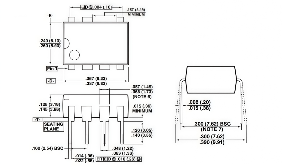
Package / Case | 8-DIP (0.300, 7.62mm), 7 Leads |
Base Part Number | TNY268 |
TNY268PN Pinout and Functional Description
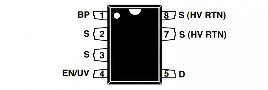
DRAIN (D) Pin:
Power MOSFET drain connection. Provides internal operating current for both start-up and steady-state operation.
BYPASS (BP) Pin:
Connection point for a 0.1 μF external bypass capacitor for the internally generated 5.8 V supply.
ENABLE/UNDERVOLTAGE (EN/UV) Pin:
This pin has dual functions: enable input and line undervoltage sense. During normal operation, switching of the power MOSFET is controlled by this pin. MOSFET switching is terminated when a current greater than 240 μA is drawn from this pin. This pin also senses line undervoltage conditions through an external resistor connected to the DC line voltage. If there is no external resistor connected to this pin, TinySwitch-II detects its absence and disables the line undervoltage function.
SOURCE (S) Pin:
Control circuit common, internally connected to output MOSFET source.
SOURCE (HV RTN) Pin:
Output MOSFET source connection for high voltage return.
TNY268PN Key Features and Benefits
TinySwitch-II Features Reduce System Cost
l Fully integrated auto-restart for short circuit and open loop fault protection – saves external component costs
l Built-in circuitry practically eliminates audible noise with ordinary dip-varnished transformer
l Programmable line undervoltage detect feature prevents power on/off glitches – saves external components
l Frequency jittering dramatically reduces EMI (~10 dB) – minimizes EMI fi lter component costs
l 132 kHz operation reduces transformer size – allows use of EF12.6 or EE13 cores for low cost and small size
l Very tight tolerances and negligible temperature variation on key parameters eases design and lowers cost
l Lowest component count switcher solution
l Expanded scalable device family for low system cost
Better Cost/Performance over RCC & Linears
l Lower system cost than RCC, discrete PWM and other integrated/hybrid solutions
l Cost effective replacement for bulky regulated linears
l Simple ON/OFF control – no loop compensation needed
l No bias winding – simpler, lower cost transformer
l Simple design practically eliminates rework in manufacturing
EcoSmart® – Extremely Energy Efficient
l No load consumption <50 mW with bias winding and <250 mW without bias winding at 265 VAC input
l Meets California Energy Commission (CEC), Energy Star, and EU requirements
l Ideal for cell-phone charger and PC standby applications
High Performance at Low Cost
l High voltage powered – ideal for charger applications
l High bandwidth provides fast turn on with no overshoot
l Current limit operation rejects line frequency ripple
l Built-in current limit and thermal protection improves safety
TNY268PN Internal Block Diagram
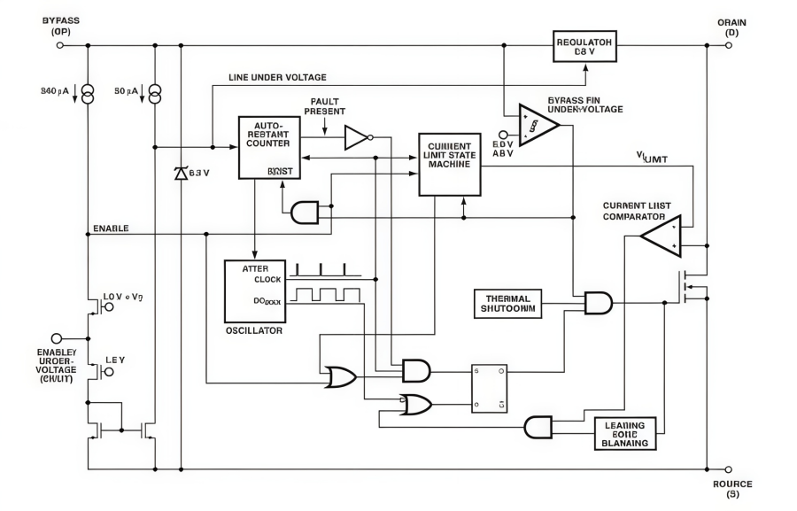
The internal 5.8V regulator draws current from the DRAIN pin to charge the BP pin, while the frequency-jittered clock and EN/UV logic control the high-voltage MOSFET in ON/OFF mode. Leading-edge blanking, current-limit comparison, auto-restart, and thermal shutdown provide simple voltage regulation and comprehensive fault protection.
TNY268PN Typical Application Circuit
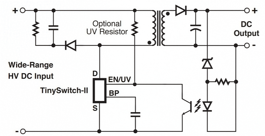
The typical application circuit uses a flyback topology. The high-voltage DC input is applied to the transformer primary winding, while the internal MOSFET at the DRAIN (D) pin controls switching. An RCD clamp circuit on the primary side absorbs leakage inductance spikes. A capacitor connected to the BP pin provides internal bypassing, while an optional high-value resistor at the EN/UV pin enables input undervoltage detection.
On the secondary side, the output is rectified and filtered, with a Zener diode and optocoupler forming the feedback loop. By pulling down the current at the EN/UV pin to skip switching cycles through ON/OFF control, the circuit provides regulated and isolated secondary-side output voltage.
TNY268PN Power Supply Applications
TNY268PN is designed for compact, low-power offline AC/DC power supplies where simple circuit design, low standby power, and integrated protection are important. Its integrated high-voltage MOSFET and control functions make it suitable for a range of consumer, industrial, and auxiliary power applications.
1. Standby Power Supplies
TNY268PN is suitable for standby power circuits that need to provide a low-power output when the main system is inactive. It can be used in equipment such as TVs, set-top boxes, home appliances, and other electronic devices.
2. AC/DC Adapters
Its integrated switching MOSFET helps simplify low-power adapter designs while reducing the number of external components. Typical applications include small consumer electronics adapters, networking equipment adapters, and auxiliary power adapters.
3. Consumer Electronics
TNY268PN can provide isolated low-voltage power for internal electronic circuits in consumer products. Examples include audio equipment, media devices, smart home products, and household electronics.
4. Industrial Control Equipment
The device can be used in auxiliary power supplies for industrial systems that require a compact AC/DC conversion stage. Applications include control panels, automation equipment, sensors, and monitoring devices.
5. Appliance Power Supplies
TNY268PN can supply low-power control circuits inside household appliances while supporting compact power supply designs. Examples include appliance control boards, timers, display circuits, and interface modules.
6. Auxiliary Power Supplies
It can generate isolated auxiliary power for control and monitoring circuits in larger systems. Typical uses include power management boards, industrial controllers, and electronic equipment with multiple power domains.
TNY268PN Protection and Reliability
TNY268PN integrates comprehensive protection features to improve power supply reliability. Its auto-restart function limits output power during short-circuit, open-loop, or feedback failures and periodically restarts operation until the fault is cleared. The thermal shutdown circuit disables switching when the junction temperature exceeds 135°C, with approximately 70°C hysteresis to prevent overheating damage.
The EN/UV pin provides input undervoltage detection and protection, while leading-edge blanking helps prevent false triggering caused by secondary rectifier reverse-recovery current. Together, these functions provide reliable protection for offline power supplies.
TNY268PN Package
ANDE Electronics: Your Trusted Partner in Electronic Component Sourcing
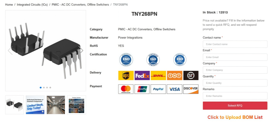
At ANDE Electronics, we make getting the electronic components you need simple and fast. We work directly with top global manufacturers to provide high-quality components that have passed our strict checks, so you can count on them for your projects.
We also focus on quick and consistent delivery to keep your work on schedule and avoid delays. When you need reliable and efficient electronic parts for your projects, ANDE Electronics is a partner you can trust.