XC7A200T-2FBG676C Overview
The XC7A200T-2FBG676C is a FPGA from the Xilinx Artix-7 family, designed with 28nm process technology to balance low power consumption and cost-effectiveness. It offers a rich set of logic resources, including over 210,000 LUTs and flip-flops. Combined with its large-capacity block RAM and 740 DSP slices, it can handle complex logic control and high-speed digital signal processing tasks.
For system integration, this FPGA provides up to 500 I/O pins that support multiple mainstream I/O standards. It also features 8 built-in GTX transceivers with a single-lane speed of up to 6.6 Gbps, making it suitable for applications that require high-speed serial communication. Its clock management is robust, with 10 integrated clock management units and a global clock network, ensuring low-latency and stable clock distribution. The device supports various configuration modes, including JTAG, SPI, and BPI, and it allows for real-time signal capture and analysis using debugging tools.
Overall, the XC7A200T-2FBG676C is an ideal FPGA solution for mid- to high-performance applications.
XC7A200T-2FBG676C Key Specs
Parameter | Value |
Part Number | XC7A200T-2FBG676C |
Description | IC FPGA ARTIX7 400 I/O 676FCBGA |
Lead Free Status / RoHS Status | Contains lead / RoHS non-compliant |
Moisture Sensitivity Level (MSL) | 4 (72 Hours) |
Base Part Number | XC7A200T |
Mounting Type | Surface Mount |
Supply Voltage | 0.95 V ~ 1.05 V |
Package / Case | 676-BBGA, FCBGA |
Number of LABs/CLBs | 16825 |
Total RAM Bits | 13455360 |
Series | Artix-7 |
Manufacturer Standard Lead Time | 15 Weeks |
Meta Part Number | 122-1865-ND |
Number of I/O | 400 |
Supplier Device Package | 676-FCBGA (27x27) |
Operating Temperature | 0°C ~ 85°C (TJ) |
XC7A200T-2FBG676C Features
Logic Resources
Logic Units (LUTs): 215,360, supporting complex logic design
Flip-Flops: 215,360, for sequential logic implementation
Block RAM: 13,140 Kb, supporting high-speed data storage and buffering
DSP Slices: 740, enabling high-performance digital signal processing (e.g., filtering, FFT)
Clock Management
Clock Management Tiles (CMTs): 10 integrated units, supporting frequency synthesis, jitter filtering, and clock division
Global Clock Network: provides low-latency and low-jitter clock distribution
I/O Interfaces
I/O Pins: 500, supporting multiple I/O standards such as LVDS, LVCMOS, SSTL
High-Speed Serial Interface: 8 integrated GTX transceivers, supporting data rates up to 6.6 Gbps
Configuration and Debugging
Configuration Methods: supports JTAG, SPI, and BPI
Debugging Support: integrated ChipScope Pro tool, supporting real-time signal capture and analysis
Power Management
Operating Voltage: core voltage 0.95V to 1.05V, I/O voltage 1.2V to 3.3V
Low-Power Design: based on 28nm process, optimized for both dynamic and static power consumption
Integration Support for the XC7A200T-2FBG676C FPGA
Development Tools
The XC7A200T-2FBG676C is fully supported by the Xilinx Vivado Design Suite, which provides a complete workflow from design entry to debugging. Developers can also take advantage of the extensive IP core library, including PCIe, Ethernet, and DDR controllers, to accelerate system integration and reduce development cycles.
Hardware Platforms
For hardware prototyping, Xilinx offers development boards such as the KC705, which are well-suited for validating designs and testing high-performance applications. In addition, a wide range of reference designs covering areas like high-speed interfaces and signal processing are available to help engineers quickly build and optimize solutions.

Software Support
This FPGA supports both VHDL and Verilog hardware description languages, making it compatible with standard digital design practices. For higher-level abstraction, it also supports High-Level Synthesis (HLS), allowing C/C++ code to be directly translated into hardware logic. The device can serve as a higher-performance alternative to models such as the XC7A100T or XC7A75T, offering improved capabilities while maintaining compatibility.
XC7A200T-2FBG676C FPGA in 4G and 5G
The Xilinx XC7A200T-2FBG676C plays a critical role in 4G and 5G wireless communication infrastructure. In 4G LTE systems, it is commonly used to implement protocol conversion and data aggregation/distribution between the BBU and RRU over interfaces such as CPRI or OBSAI. It can also execute specialized digital signal processing algorithms, including DPD and CFR, to improve power amplifier efficiency or serve as a baseband co-processor in small cell deployments.
As networks evolve toward 5G, the demands for bandwidth, latency, and flexibility increase dramatically. In this context, the XC7A200T has found more strategic applications. It is well-suited for deployment in 5G Distributed Units and Radio Units to implement portions of the physical layer, such as precoding and beamforming algorithms in massive MIMO systems, as well as efficient fronthaul transmission and offloading via interfaces like eCPRI.
Its high-speed transceivers can directly handle the high data rates required for millimeter-wave bands, providing a critical programmable hardware platform for 5G macro and small cells, as well as early prototyping and test equipment, effectively accelerating 5G technology development and deployment.
XC7A200T-2FBG676C Use Cases
1. Communication Equipment
XC7A200T-2FBG676C, with its high-speed serial transceivers and powerful parallel processing capabilities, has become a core component in the field of communication devices.
l Wireless Base Stations: used for baseband processing and signal modulation.
l Network Equipment: enables high-speed packet processing and protocol conversion.
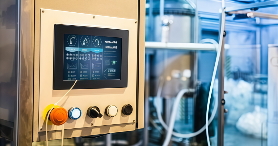
2. Industrial Control
In industrial control, which requires high reliability and determinism, this FPGA performs excellently.
l Motion Control: used for multi-axis servo control and robotic control.
l Data Acquisition: enables high-speed data acquisition and real-time processing.
3. Medical Devices
Medical devices demand high precision in signals and real-time processing; XC7A200T provides an ideal solution.
l Medical Imaging: used for image processing in CT, MRI, and similar equipment.
l Vital Signs Monitoring: enables multi-channel signal acquisition and analysis.
4. Consumer Electronics
In the field of consumer electronics, this chip provides strong performance support for high-end applications.
l Video Processing: used for 4K video encoding and decoding.
l Gaming Devices: enables high-performance graphics rendering and physics simulation.
Comparison with Other Xilinx 7-Series FPGAs
The XC7A200T-2FBG676C, part of the Artix®-7 Family, is optimized for low-power applications that require high DSP and logic throughput along with integrated serial transceivers. It can provide a cost-effective solution for high-throughput, performance-sensitive designs.
Compared to the Spartan®-7 Family, which prioritizes the lowest cost and very small form-factor packaging, the Artix-7 devices like XC7A200T offer higher logic density, more DSP slices, and advanced serial transceivers while still maintaining low power consumption.
Relative to the Kintex®-7 Family, which focuses on the best price-to-performance ratio and roughly doubles performance compared to previous generations, the Artix-7 series balances performance and cost for mid-to-high throughput applications without the higher cost of Kintex devices.
Compared to the Virtex®-7 Family, which is designed for maximum system performance and capacity with stacked silicon interconnect (SSI) technology, the Artix-7 series delivers lower total system cost while providing sufficient logic, memory, and I/O resources for most high-throughput yet cost-sensitive applications.
FAQs about XC7A200T-2FBG676C FPGA
What is the XC7A200T-2FBG676C?
It is a high-performance FPGA from Xilinx’s Artix®-7 family, built on 28nm technology, offering high logic density, DSP capability, and serial transceivers for cost-sensitive, low-power applications.
What are its key resources?
It features 215,360 LUTs and Flip-Flops, 13,140 Kb of block RAM, 740 DSP slices, 500 I/O pins, and 8 GTX high-speed transceivers supporting up to 6.6 Gbps.
What applications is it suitable for?
Common uses include communication equipmen, industrial control , medical devices and consumer electronics.
ANDE Electronics: Your Trusted Partner in Electronic Component Sourcing
At ANDE Electronics, we make electronic component sourcing simple, efficient, and tailored to your specific needs. Through long-standing partnerships with leading global manufacturers, we provide high-quality components that meet strict inspection and verification standards, ensuring your projects stay reliable.
We also focus on speed and consistency: our prompt delivery keeps your workflows on track and minimizes delays. For efficient, customized electronic component sourcing you can rely on, ANDE Electronics is your trus